AI Chip Design in Nine Months: What OpenAI's Jalapeño ASIC Proved
OpenAI's Jalapeño chip went from design code to tapeout in nine months. Here is what AI actually did, and what people still had to do.

In this article 6 sections
OpenAI's Jalapeño ASIC went from register-transfer level (RTL) design to tapeout in nine months, about half the usual 18 to 24 months. AI chip design did much of that work, because OpenAI's own models, mostly Codex, helped write designs and kernels. Humans still made the architecture calls, and standard tools still signed off the silicon.
This post explains what OpenAI built, how the schedule shrank, and which parts of chip design AI really handles today. It is written for engineers, IT buyers, and anyone who has to judge a vendor's "AI-designed chip" pitch. At Protocol Wire, we cover AI hardware and software.
What Did OpenAI Actually Build With Jalapeño?
Jalapeño is an application-specific integrated circuit (ASIC) for AI inference, built by OpenAI's new hardware team. An ASIC is a chip built for one job instead of many. This one was designed from a blank page, with no legacy code to reuse, and it was shown at Hot Chips 2026.
Richard Ho, OpenAI's head of hardware, said in an interview with Tom's Hardware that the team had "nothing" to start from. The usual baseline for a chip like this is 18 months to two years, and that often includes some existing IP. Jalapeño went from concept to reveal in under two years.
The chip is not a one-off. OpenAI says its second-generation ASIC is approaching tapeout, and a third generation is already in development. That fits a wider shift toward custom silicon, which we covered in our look at the chips powering this year's AI boom.
The first stepping, called A0, was not the final word. The B0 stepping reportedly delivers up to 25% better performance per watt. That is closer to a generational jump than a routine fix, which hints at early design oversights from a brand-new team.
Whether AI or people caused those oversights is anyone's guess. OpenAI has not split the blame, and we would not trust anyone who claims to know. What the number does show is that first silicon from a new team still needed a real respin.
How Did AI Chip Design Get Down to Nine Months?
OpenAI used its own models, mostly Codex, to write and check design code, then to write the software kernels that run on the chip. A small group of strong engineers steered those models. The models also improved sharply during the project, which sped up the later stages.

Ho said the work began in November 2025. By the time the team started kernel optimization in May, when the first chips came online, he said the team was "shocked" at how much better Codex had become. A tool that improves mid-project changes the math on any schedule.
The team also co-designed the chip with OpenAI's software stack. That matters because a chip is only useful when software can use it. Writing kernels, the low-level routines that run math on the hardware, is often where a new accelerator stalls.
In tape-out postmortems, the schedule rarely slips in the first draft of a design. It slips in the loop between finding a bug and proving the fix works. Agents are strongest in that loop, because a simulation gives a fast, concrete pass or fail.
The feedback loop here is worth spelling out. Today's AI models run on chips that engineers designed with growing help from AI. Those models now help design the next chips. That loop is why the industry asks how fast it can tighten, and what AI infrastructure costs.
Ho also said the old approach was not the only bottleneck. Existing teams often start with legacy architecture, which speeds some work and slows other work. A blank page gave OpenAI freedom, and it cost the team a lot of early decisions that a veteran chip company would have inherited.
Ho was blunt about the human role. "We didn't replace our engineers; they just became super productive," he said. It is one of the few clear examples of AI boosting a team instead of shrinking it.
Which Parts of Chip Design Can AI Handle Today?
AI handles the most work in front-end design and verification, where RTL, testbenches, and assertions are all code. It also helps with physical layout tasks like floorplanning, placement, and routing. It does not yet own architecture decisions or final signoff, which stay with engineers and proven tools.
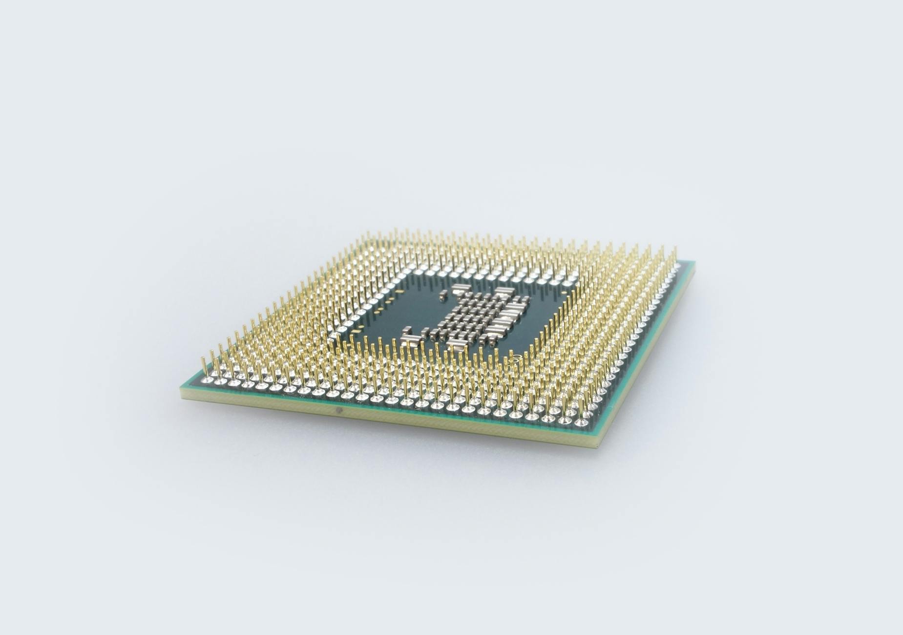
The layout side has the longest track record. Google DeepMind says AlphaChip has produced chip layouts for its last three generations of Tensor Processing Units (TPUs). The company says those layouts arrive in hours instead of the weeks or months of human effort.
The table below maps each stage of chip design to the role AI plays as of September 2026.
| Design stage | What AI does today | Example |
|---|---|---|
| Floorplanning | Places circuit blocks using reinforcement learning | Google AlphaChip |
| Placement and routing | Searches options to hit power, speed, and area goals | Cadence and Synopsys tools |
| RTL and verification code | Writes and revises code, then runs simulations in a loop | OpenAI Jalapeño |
| Failure triage | Reads reports and proposes fixes | Agentic EDA tools |
| Signoff | Not replaced; standard engines check the result | Timing and signal integrity analysis |
| Architecture | Humans define what the chip does | Jalapeño design team |
The first wave of AI in electronic design automation (EDA) software, the tools engineers use to design chips, relied on machine learning to optimize a design that humans had already defined. The newer wave writes code and runs tools on its own. That is a real change in who does the work.
Front-end work is where the gains are largest, and the reason is simple. RTL, testbenches, and assertions are all code, so language models can read and write them. Simulations return fast pass-or-fail answers, which lets agents run many checks in parallel instead of waiting on a person to review each report.
Not every claim holds up, though. In late August, a startup called Architect Labs said it had built a chip almost entirely with AI. That would be an industry first, but the claim is the company's own, and we have not seen independent verification. Until then, "almost entirely" is a marketing phrase, not an engineering result.
Signoff and Architecture Still Belong to Humans and Proven Tools
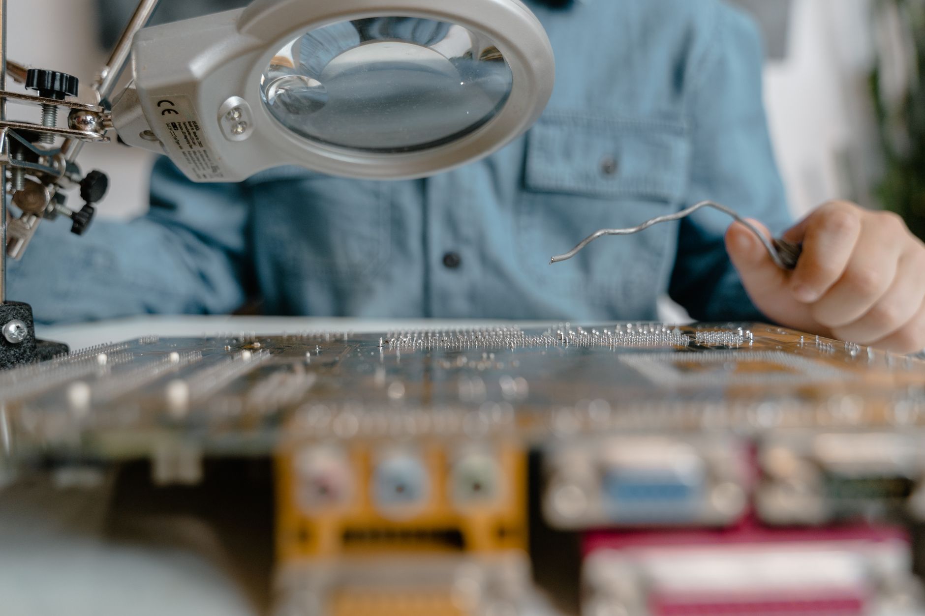
OpenAI did not skip the traditional checks. Before tapeout, the point where a final design is sent for manufacturing, the team ran standard EDA flows for static timing analysis and signal integrity analysis. Ho said there is "no real alternative today" for signoff.
The team also made pragmatic trade-offs early. It avoided emerging, complex design points like 3D stacking and co-packaged optics. That is one reason nine months was possible, and Ho said other chips will not necessarily follow the same timeline.
Vendor claims deserve the same care. In Tom's Hardware's review of agentic EDA tools, Cadence described a demo as "bounded Level 5 in one domain," while saying most of its agent technology sits at an advanced Level 4. Those levels are vendor-defined marketing ladders, not an industry standard.
The speed numbers have the same problem. Most gains come from the vendors or their customers, and they measure different tasks against different baselines. In one example, Empyrean says an agent cut a layout task from four weeks to one. Without a shared benchmark, none of these figures can be compared.
As a rule, a claim like "AI designed this chip" is nearly always a claim about one stage. Ask which stage. Then ask who signed off the result.
What Buyers and Engineering Teams Should Take From This

Ho does not expect nine-month cycles to repeat back to back. He said he does not want to tape out something only 2% better than the last chip, because changing out a fleet costs too much. The technology also has to be ready for each new cycle.
For buyers, the near-term effect is more custom silicon and more competition for merchant GPUs. That connects to how AI chip procurement is changing, where supply, not just speed, decides who gets capacity. Talent is moving too, since a key Jalapeño engineer left OpenAI in June to join Anthropic's hardware team.
When a vendor pitches AI-designed silicon, ask three questions:
- What baseline did you measure the schedule savings against?
- Which stages did AI touch, and which did standard signoff tools check?
- Is this first silicon or a later stepping, such as B0 instead of A0?
Engineering teams can take a lesson from the process. A small team of experts, strong tooling, and fast simulation loops beat a large team working serially. That advice applies well beyond chips. Teams that shorten the loop between a failed test and a verified fix will ship sooner, whether they build silicon or software.
The Bottom Line on AI Chip Design
Jalapeño shows that AI chip design can cut a schedule roughly in half when a strong team drives it. It does not show that chips now design themselves. Architecture and signoff stayed human and proven.
Treat every speed claim as a claim about one stage, on one baseline, from one vendor. Watch the second-generation tapeout next. Protocol Wire will keep tracking it. If OpenAI repeats the result with a less blank-page design, the new baseline is real.